
Site Directory:
Step by Step Flyback SMPS Design by Prasun Kulshrestha |
Abstract: The approach of this article is to develop a sequential approach of practically designing the SMPS design Which are examined by me for years practically. The aim is to look on ground levels to clear fundamentals intelligence regarding SMPS. I had never seen Easy & step- by-step calculations to ideally decide the nature of SMPS. The Step-by-step calculations illustrated in this article will help you to actually see the practical result on paper before performing it practically. This also include the expertise tips wherever it is desired for either caution or for intelligence.
Moreover, when you will make the actual schematic using these calculations, you will just need a perfect guidance for implementing correct component data book. I was also looking to include the probable components that could be referred but finally I am not including it in this.
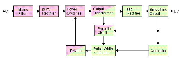
Universal Block Diagram :

Fig: Pras:1
Introduction:
Designing the system step-by step could be realized below. Moreover the block diagram above is a self-explanatory Universal block diagram of SMPS.
I had enlisted the Sequential formulas below which will clear the insight towards SMPS.
A.Step by step Designing Formulas:
If No information is available , just assume Eff=0.75 for low output applications & 0.85 for high voltage applications.
Pin = Po / E ff
Put Eff = as discussed above.
Now, if we have to take multiple outputs from smps,the load occupying factor ( KLn) must be found as-
KLn=Po(n)/Po
Here, Po(n) is the maximum output power for nth output.
Usually, if single output from smps is desired, key rule is to consider KL = 1
3.Input capacitor Selection:
It is also known as DC link capacitor.
The universal approach should be to first recognize the few parameters as :
Vac max; Vac min ; switching frequency ; line frequency & output power;
This would clear the nature of quality of an ideal SMPS you are looking at.
The key rule to decide the value of Dc link capacitor as 2-3 micro farad per watt of input range ( 85-265vrms) & 1 micro farad per watt of input power of European range ( 195v -265vrms)
Also, take my experience suggestion to use DC link capacitor more than 2 micro farad per watt of input range so as to get better quality of DC output.
Also, for 230 v mains line, select the capacitor of min 400 v rating. It is because that we may use rectifier device which may multiply the input with the factor of 1.41.
Vdc min = sprt( 2* ( v line min )^2-Pin ( 1-Dch )/ Cdc. Fl )
Where ,
Dch- dc link capacitor charging duty ratio.
Dch is 0.2 to 0.25
Dch = t1 /t2
Vdc max = sqrt (2 )* V line max
Change in Vdc max = sqrt (2) * Vlin min – V dc min
While calculating this factor, care should be taken as accuracy of this factor affects the system a lot.
Vro = Dmax* Vdc min / (1- Dmax)
Vds nom = Vdc max +Vro
Where Vdc min & Vdc max is already calculated in step 3 & 4.
Practical approach key rule:
For step 6 & 7;
If we decrease the value of Dmax, the voltage stress over MOSFET can be reduced suitably. But this will in turn increase the voltage stress over rectifier diode in the secondary side. So, I would suggest with my experience to Select Dmax as large as possible if the voltage rating of MOSFET allows.
8.Designing The inductance of the transformer primary side Lm:
Lm= (Vdc min * Dmax)square / (2 Pin * Fs * Krf)
Where Lm- primary inductance
F s- switching frequency
Krf- ripple factor in full load & min input voltage.
Key rule:
For discontinuous mode , set krf =1
For continuous mode, set kef < 1
If you are making flyback converter to be operated in CCM mode, just prefer to set krf between 0.25 – 0.5 for universal input range & krf = 0.4 – 0.8 for European input range.
9 Ids peak = I edc + ( Change in current / 2)
10. Ids rms = sqrt((3* (Iedc)square + ( change incurrent / 2 )square)Dmax / 3 )
11. where Iedc = Pin / (Vdc min * Dmax)
12. Also, change in current = Vdc min * D max / (Lm* Fs)
13. Vdc in ccm mode = [1/(sqrt(2*Lm*fs*Pin))-1/Vro]^(-1)
Key rule:
If the result of equation 13 is in negative value, the converter is always in CCM under full load condition regardless of the input voltage variation.
14. Np (min) =[ Lm* Ilim * 10^(6) / ( Bsat * Ae)] (turns)
Where Ilim – pulse by pulse current limit level
Ae = cross section area of the core
Bsat = saturation flux density in tesla
Key rule: if no information is available regarding Bsat,for generalized smps, set Bsat between 0.3 to 0.35 tesla
15. Transformer design
n = [Np/Ns1] =[Vrd/ ( V01+Vf1 )]
where Np- number of turns of primary side
Ns1- number of turns of reference output
V01 – output voltage
VF1 – Diode forward voltage drop of the reference output .
Key suggestion:
Now, determine the proper integer number for NS1 so that resulting Np is larger than Np min Obtained from step 14.
16. The number of turns for the other output , nth output, is determined as:
Ns (n) = [ V0 (n) + Vf(n)* Ns1] / [ V01 +Vf1 ] turns
17. The number of turns for V0c winding is determined as :
Na = [ Vcc + Vea /( V01 + Vf1 ) ] * Ns1 turns
Where Vcc – nominal voltage for Vcc.
Vfa- Diode forward voltage drop.
18. with determing turns of the primary side, the gap length of the core is obtained as :
G = 40* 3.14 * Ae [ {Np^(2)/ 1000Lm}-1/Al ] units in mm
Where Al- Al value with no gap in nH/turns^(2)
Ae = Cross section area of the core.
Np = no. of turns for primary side of the transformer.
19: The RMS current of the nth secondary winding is obtained as :
I sec (n)rms = I ds rms sqrt [ (1-Dmax/Dmax)] * Vro * Kln / { Von + Vf n }
Where Von – output voltage of nth output
V fn – diode forward voltage drop
Kln – load occupying factor for nth output defined in equation 2.
Key information:
The current density is 5A / mm2 when the wire is long (> 1m). when the wire is short with a small number of turns , a current density of 6-10 A/mm is also acceptable.
Avoid using wire with a diameter larger than 1mm to avoid severe eddy current losses as well as to make winding easier.
For high current output, it is better to use parallel winding with multiple strands of thinner wire to minimize skin effect.
19. The required winding window area is given by :
Aw = Ac / Kf
Where Ac – actual conductor area
Kf = Fill factor
Key tip:
Usually, fill factor is in between 0.2 to 0.25 for single output application.
For, multiple output, it is in between 0.15 to 0.2.
20. The maximum voltage & the rms current of the rectifier diode of the nth output are obtained as :
Vdn = V0n + Vdc max [ V0n + Vfn ] / Vro
21: Idn rms = Ids rms sqrt ( 1- Dmax /Dmax ) * Vro * Kln/ ( Von + Vfn )
where von – output voltage of nth output
vfn- diode forward drop.
22. The typical voltage & current margins for rectifier diode are as follows:
Vrrm > 1.3 * Vdn
23. I f > 1.5 * I dn rms
where ,
for equation 23 & 23,
Vrrm – maximum reverse voltage
I f – average forward current of diode.
Trr- maximum reverse recovery time.
24. The ripple current of the nth output capacitor C0n is obtained as :
I cap n rms = sqrt [ ( Id n rms) square – Io (n)square ]
Where
Io (n) – load current of the nth output
Idc n rms – equation 21.
25. the voltage ripple on the nth output is given as :
change in Von = [Ion/(Con*Fs)] + [ Tds peak * V ro * Rcn * Kln] / [ Von + Vfn ]
where:
Con- capacitance
Ron- effective series resistance ESR, of the nth output capacitor.
Ion – load current
Von- output voltage
Vfn – diode forward voltage
Key tip: IMPORTANT
If we use single output capacitor, with high ESR, it is possible to meet ripple specification . If further required, use additional lc filter stages (post filter). When using post filter, be careful not to place the corner frequency too low. Too low corner frequency make the system unstable or limit the control bandwidth. It is typical to set the corner frequency of the post filter around 1/10 to 1/ 5 of the switching frequency.
26: Snubber design
designing a snubber circuit is a vast field for calculations & implementations. But, the key formula is as below:
Psn = Vsn ^(2)/ Rsn = ½ [ Fs* Lik * (Ids peak)^(2)*Vsn/ (Vsn-Vro) ]
Where
Ids peak – refer equation 9
Fs – switching frequency
Lik – leakage inductance
Vsn- snubber capacitance voltage At min i/p v & full load.
Vro- reflected output voltage
Rsn- snubber resistor
Key tip:
Vsn should be greater than Vro & It is typical to set Vsn To be 2 to 2.5 times of Vro. Too small Vsn results in a severe loss in the snubber network as shown in equation 26.
· The leakage inductance is measured at the switching frequency with all other windings shorted.
27. The maximum ripple of the snubber capacitor voltage is obtained as :
Change in Vsn = Vsn1/ ( Csn * Rsn * Fs)
Key information:
In general, 5 to 10 % ripple is reasonable. Use better quality capacitor, I would recommend it because high voltage spike affects the performance of Capacitor, so poor quality capacitor would be a worst option to use in such case.
28. Snubber capacitor Voltage under maximum input voltage & full load condition is obtained as :
Vsn2 = Vro + Sqrt ( (Vro)^(2) + 2 Rsn * Lik * Fs * I ds2 ^ (2) / 2
Where Lik – primary side leakage inductance
Vro – reflected output
Voltage
Rsn – snubber resistor
Ids 2 – Peak drain current at the maximum input voltage & full load condition.
29: If the converter is operated in CCM mode, at the maximum input voltage & full load condition , for equation 28,
I ds2 = [Pin (Vdc max + Vro)/ ( Vdc max * Vro)] + Vdc max * Vro/ [ 2Lm * Fs * ( Vdc max + Vro ) ]
30: If converter is operated in DCM at maximum input voltage & full load condition :
Ids2 = Sqrt (2*Pin/ Fs* Lm)
31: Maximum voltage stress on the internal MOSFET is given by :
Vds max = Vdc max + Vsn2
Key tip:
Check if Vds max is below 90% of the rated voltage of MOSFET Bvdss . The voltage rating of snubber diode should be higher than BVdss.
Usually ultra fast diodes with 1A current rating is used for snubber circuit.
32: Feedback calculations
32-A: Please consider few restrictions while calculating feedback elements.
The voltage divider network of R1 & R2 should be designed to provide 2.5 to the reference pin of LM431/ Tl 431/ Ka431
Rf = 2.5 * R1/ [V01 – 2.5]
Where Vref = reference output voltage of Lm431.
32-B:
The Rbias & Rd used together with the opto coupler & the shunt regular LM431 should be designed to provide proper operating current for the LM431 & to guarantee the full swing of the feedback voltage for switching device used.
In general , the minimum cathode voltage & current for the LM431 are 2.5 & 1mA. Respectively.
Therefore, Rbias & Rd should be designed to satisfy the following conditions.
32-C
[ Vout-Vop-Vref / Rd ] > Ifb
32-D
Vop/ Rbias > 1 mA
Where Vout – voltage supplying LM431
V op- Opto coupler forward drop
33: The current control factor of Power switch ‘ k ‘ is defined as :
k = Ipk/ Vfb = I over / Vfb sat
where , I pk – peak drain current
Vfb – Feedback voltage
I over – current limit
Fbsat – feedback saturation voltage typically 2.5
34: For CCM operation, the control to output transfer function of the flyback converter using current mode control is given by :
Gvc = [ V01/ V fb ]
= [K* Rl*Vdc (Np/NS1)/2V*Ro][ (1+ S/w2)(1-S/w2)/ 1+(S/wp)]
where Vdc – input voltage
Rl – effective load resistance of controlled output.
The pole & Zeros of step 34 are as :
W2 = 1/ RC1* Co1 ;
Wr2 = (1-D)^(2)/[D * Lm * (NS1 /Np)^(2)
Wp = {1+D/ Rl * Co1}
35: For DCM operation :
Gvc = V01/ Vfb = [Vo1/ VFB][ {1+S /w2}/ ( 1+ S/wp )
Where w2 = 1/ Rc1* Co1
Wp = 2/ [ Rc1* Co1 ]
36: The feedback Compensation network transfer function is defined as :
Gvc = Vfb = -[Wi/s][ ( 1+s/w2c)/ ( 1+1/Wpc ) ]
Where ;
Wi= Rb/ [ R1*Rd* Cf ]
W2c = 1/ [ (Rf+R1)*Cf]
Wpc = 1/ [Rb* Cb]
Feedback bias resistor
|
37: T delay = (Vsd – 2.5) Cb/I delay |